


Diodes Incorporated PI6C492150xTQ Automotive LVDS Buffer Outputs
Diodes Incorporated PI6C492150xTQ Automotive LVDS Buffer Outputs feature low delay from input to output and separate input-output supply voltage for level shifting. These devices are ideal for systems that distribute low-jitter clock signals to multiple destinations. The PI6C492150xTQ LVDS buffer outputs are AEC-Q100 qualified, lead-free, and fully RoHS compliant and support automotive grade 1. These LVDS buffer outputs feature 2/4 LVDS outputs with 2 banks and LVCMOS reference output up to 200MHz. The PI6C492150xTQ LVDS buffer outputs operate at -40°C to 125°C ambient temperature range and 150°C junction temperature (max). These LVDS buffer outputs are ideally used in networking systems, including switches, routers, and automotive infotainment.
Features
- 2/4 LVDS outputs with 2 banks
- Selectable reference inputs support either single-ended or differential or Xtal
- <40ps low skew between outputs within banks
- Low delay from input to output
- Separate input-output supply voltage for level shifting
- AEC-Q100 qualified, automotive grade 1 support
- Lead-free and fully RoHS compliant
- Halogen and antimony free
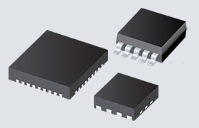
- 32-pin WQFN (ZHW) packaging
Specifications
- Up to 200MHz LVCMOS reference output
- -40ºC to 125ºC ambient temperature range
- Up to 1.5GHz output frequency for differential outputs
- -55ºC to 150ºC storage temperature range
- 150ºC junction temperature (max)
Applications
- Networking systems, including switches and routers
- High-frequency backplane-based computing and telecom platforms
- ADAS
- Automotive infotainment
Block Diagram

Package Mechanical Diagram

Published: 2023-07-24
| Updated: 2023-08-18