


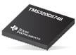
Texas Instruments TMS320C6452 Digital Signal Processor (DSP)
Texas Instruments TMS320C6452 Digital Signal Processor (DSP) is a high-performance fixed-point DSP generation in the TMS320C6000™ DSP platform. The C6452 device is based on the architecture of third-generation, high-performance, and advanced VelociTI™ Very-Long-Instruction-Word (VLIW). This device performs up to 7200 Million Instructions Per Second (MIPS) at a 900MHz clock rate. The TMS320C6452 DSP features a 3-Port Gigabit Ethernet switch subsystem, two Telecom Serial Interface Ports (TSIP0/1), and one UART (with RTS and CTS Flow Control). This device is ideal for medical diagnostics, machine vision/inspection, radar and sonar, military/aerospace, and communications.
Features
- High-performance digital media processor:
- 720MHz, 900MHz C64x+™ clock rates
- 1.39ns (-720) and 1.11ns (-900) instruction cycle time
- 5760, 7200 MIPS
- Eight 32-bit C64x+ instructions/cycle
- Fully software-compatible with C64x/debug
- Commercial temperature ranges (-720 and -900 only)
- Industrial temperature ranges (-720 and -900 only)
- VelociTI.2™ Extensions to VelociTI™ Advanced Very-Long-Instruction-Word (VLIW) TMS320C64x+™ DSP Core:
- Eight highly independent functional units with VelociTI.2 extensions:
- Six ALUs (32-/40-bit), each supports single 32-bit, dual 16-bit, or quad 8-bit arithmetic per clock cycle
- Two multipliers support four 16 x 16-bit multiplies (32-bit results) per clock cycle or eight 8 x 8-bit multiplies (16-bit results) per clock cycle
- Load-store architecture with non-aligned support
- 64 32-bit general-purpose registers
- Instruction packing reduces code size
- All instructions conditional
- Additional C64x+™ enhancements:
- Protected mode operation
- Exceptions support error detection and program redirection
- Hardware support for modulo loop Auto-Focus module operation
- Eight highly independent functional units with VelociTI.2 extensions:
- C64x+ instruction set features:
- Byte-addressable (8-/16-/32-/64-bit data)
- 8-bit overflow protection
- Bit-field extract, set, and clear
- Normalization, saturation, and bit-counting
- VelociTI.2 increased orthogonality
- C64x+ extensions:
- Compact 16-bit instructions
- Additional instructions to support complex multiplies
- C64x+ L1/L2 memory architecture:
- 256K-bit (32K-byte) L1P program RAM/Cache (direct mapped)
- 256K-bit (32K-byte) L1D data RAM/Cache (2-way set-associative)
- 1408KB L2 unified mapped RAM/Cache (flexible allocation)
- Supports Little Endian mode only
- External Memory Interfaces (EMIFs):
- 32-bit DDR2 SDRAM memory controller with 512M-byte address space (1.8V I/O)
- Asynchronous 16-bit wide EMIF (EMIFA):
- Up to 128M-byte total address reach
- 64M-byte address reach per CE space
- Glueless interface to asynchronous memories (SRAM, Flash, and EEPROM)
- Synchronous memories (SBSRAM and ZBT SRAM)
- Supports interface to standard sync devices and custom logic (FPGA, CPLD, ASICs, etc.)
- Enhanced Direct-Memory-Access (EDMA) controller (64 independent channels)
- 3-Port Gigabit Ethernet switch subsystem
- Four 64-bit general-purpose timers (each configurable as two 32-bit timers)
- One UART (with RTS and CTS flow control)
- One 4-wire Serial Port Interface (SPI) with two chip-selects
- Master/Slave inter-integrated circuit (I2C Bus™)
- Two Telecom Serial Interface Ports (TSIP0/1)
- Multichannel Audio Serial Port (McASP):
- Ten Serializers and SPDIF (DIT) mode
- 16/32-bit Host-Port Interface (HPI)
- Advanced Event Triggering (AET) compatible
- 32-bit 33-/66MHz, 3.3V Peripheral Component Interconnect (PCI) Master/Slave interface conforms to PCI specification 2.3
- VLYNQ™ interface (FPGA interface)
- On-chip ROM bootloader
- Individual power-saving modes
- Flexible PLL clock generators
- IEEE-1149.1 (JTAG™) Boundary-Scan-Compatible
- 32 General Purpose I/O (GPIO) pins (multiplexed with other device functions)
- Package:
- 529-pin nFBGA (ZUT suffix)
- 19mm x 19mm, 0.8mm pitch BGA
- 0.09µm/6-Level Cu Metal Process (CMOS)
- 3.3V and 1.8V I/O, 1.2V internal (-720 and -900)
Applications
- Medical diagnostics
- Machine vision/inspection
- Radar and sonar
- Military/aerospace
- Communications
Related Products
Texas Instruments TMS320C6748 Fixed & Floating-Point DSP
Offers low-power applications processor based on a C674x DSP core.

Texas Instruments TMS320C672x Digital Signal Processor
High-performance, 32-/64-bit floating-point DSP with an enhanced C67x+™ DSP core.

Texas Instruments TMS320C665x Fixed & Floating Point DSPs
High performance fixed and floating-point DSPs based on TI's KeyStone multicore architecture.
Functional Block Diagram
")
Published: 2024-05-02
| Updated: 2024-06-16